Electrical Design
The WISPR electrical design builds upon the SoloHI development program and consists of two major components: the Camera Electronics (CE), provided by NRL, and the Instrument Data Processing Unit (IDPU), provided by the Johns Hopkins University/Applied Physics Laboratory (JHU/APL). Each component comprises several subsystems, which we describe briefly below.
Camera Electronics
The WISPR Camera Electronics control and read out the APS detectors for both telescopes and send raw camera images to the IDPU for processing. They consist of the Camera Interface Card (CIC), which communicates between the IDPU and the two telescopes, and the image acquisition circuitry for the two telescopes. The latter comprises the APS detector, the Detector Interface Board (DIB) and the Detector Readout Board (DRB) enclosed within the FPA for each telescope (Fig. 10).
Camera Interface Card
The CIC provides the electrical interface to the IDPU, routing of command/telemetry within the instrument, coordination of the inner/outer telescope readouts, signal chain and 14-bit A/D conversion of video from the two telescopes, and local analog telemetry acquisition. An RTAX1000SL FPGA provides the logic for the CIC. The CIC supports a Camera Link Interface (CLI) to GSE for early testing, and an interface to the IDPU, which provides: (1) a Command/Telemetry serial interface with 3.3 V LVDS async UART 19.2k BAUD, and (2) a serial pixel interface (SPI) with LVDS interfaces for serial header and video, 40MHz clock, and DVAL/LVAL/FVAL signals sent to the IDPU. The SPI supports a 2 Mpixels/sec readout with a ≤256 bytes header.
Active Pixel Sensor
The WISPR imaging detector is based on the Active Pixel Sensor (APS) developed by Sarnoff Corporation for the SoloHI investigation (Fig. 21). Table 5 summarizes the WISPR APS imaging specification. The detector is radiationhardened (operational after >1 Mrad exposure), has excellent performance in read noise, dark current, and full well capacity, and simplifies the drive electronics compared to CCDs. The APS detector includes the readout preamplifiers, the Double Correlated Sample and Hold circuitry, multiplexers and switches to access and read individual pixels. The capability to access individual pixels nearly eliminates the charge transfer efficiency (CTE) degradation from radiation damage and the image smearing in shutterless operation, present in the SECCHI/HI images. The device can operate under two gain modes: a high gain mode with full well >120,000 e− and ∼40 e− read noise, and a low gain mode with full well >20,000 e− and ∼7 e− read noise.
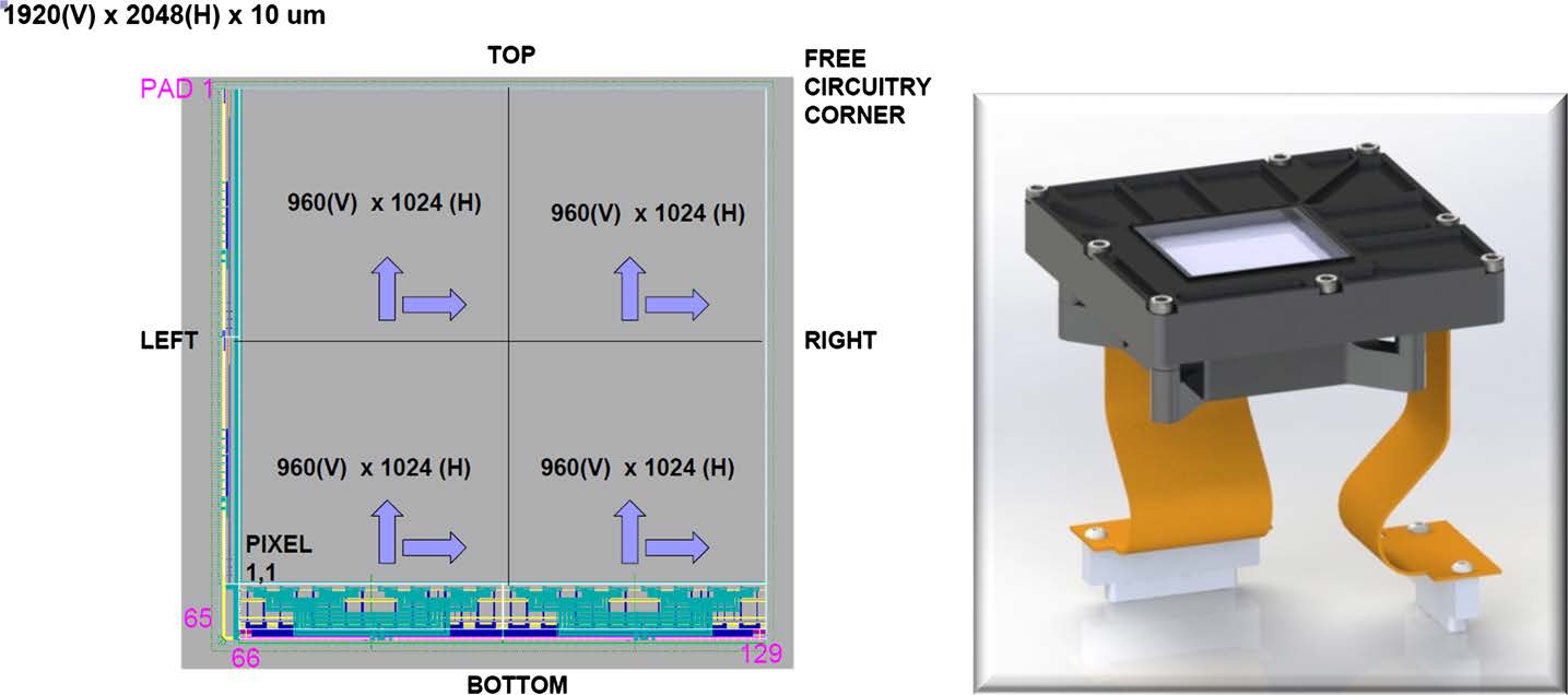
Right: The APS/DIB flight package. The two yellow flex cables connect the sensor to the DRB
WISPR APS Detector Performance Capability
| Parameter | Capability |
|---|---|
| Format | 2048×1920 |
| Pixel (size, type) | 10 μm, 5T PPD |
| Operating Temperature Range | <−55 ◦C |
| Technology | Jazz 0.18 μm |
| Power | <500 mW at 3.3 V |
| QE | >34.3 % average over 470–755 nm |
| Radiation Tolerance | Tested to 100 Krad |
| Read Noise (EOL, 95 % of pixels) | 7–13 e−/pix |
| Dark Current (EOL, 95 % of pixels) | 1.57–1.9 e−/s/pix |
| Linear Full Well (95 % of pixels) | 20,000–21,300 e−/pix |
| Readout Rate | 2 Mpix/s |
| Digitization | 14-bit ADC |
| Cosmetics | 95 % of pixels meet EOL requirements |
| Readout Modes | Progressive scan, global reset |
| Redundancy | Independent operation of each 960 ×2048 half |
The WISPR APS detector utilizes the detector designs developed by the Solar Orbiter SoloHI program. The pixel design had been advanced in a series of ‘sandbox’ test runs under a Sarnoff development program (Korendyke et al. 2013). The performance of the detectors before and after radiation has been evaluated and documented during the SoloHI development program. The result of these tests raised the maturity level to TRL 6. To minimize dark current and potential radiation damage, the detectors will operate at moderately low temperatures (<−55 ◦C) using a cold finger passive radiator. The flight device fabrication has been completed and the selection and burn-in of flight candidates is underway. The WISPR program requires at least 4 flight devices (2 flight models and 2 flight spares).
Detector Interface and Readout Boards (DIB/DRB)
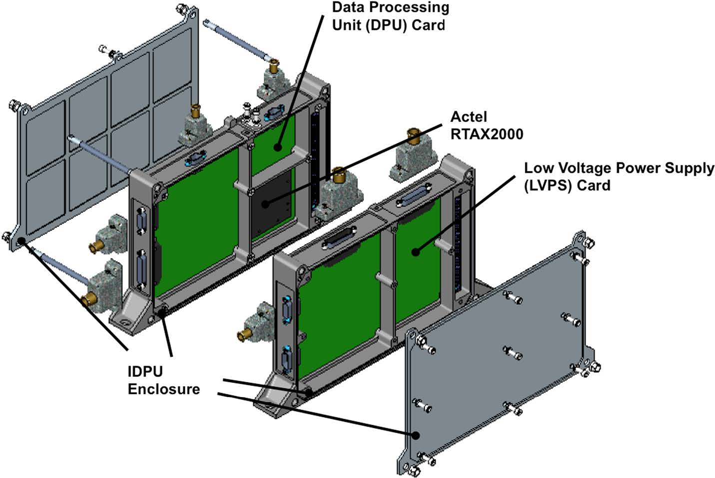
The DRB generates the readout sequencing and collects the raw video from the DIB, sets the (adjustable) bias signals for the APS, monitors the detector temperature and controls the operation of the calibration LEDs. An RTAX1000SL FPGA provides the logic for the DRB.